User Tools
Sidebar
This is an old revision of the document!
Analog Cherry Keyboard Attempt 3 (WIP)
After a while of looking at it, this seems far too complicated! There have to be simpler, cheaper, and more accurate solutions. I started searching for some ICs that maybe can do the trick but didn't found any good other than the links I posted above. But then Henrik found something great: The LDC1314
It is really good…I think.
https://www.ti.com/lit/ds/symlink/ldc1314.pdf?ts=1594984537226
And ti even has an informative paper about PCB-Coils and LDC Sensor Design: https://www.ti.com/lit/an/snoa930b/snoa930b.pdf?ts=1594984818448 Important Pages:
- 7-9
On it goes with designing a real PCB. The Milled CBs are just not accurate enough for this kinda task. Some cheap prototype PCBs from China have to be used. Maybe I should think about selling these when I´m finished. Getting kinda pricy. ( :thinking: about Best Idea Cup (maybe not because it's not my idea))
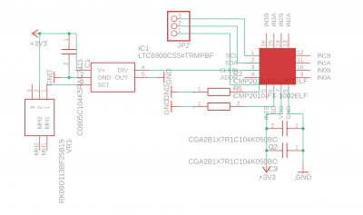
This is the current state. The PCB Coil is still missing. Have to do some calculations. Btw I´m now using Eagle! This is so much more comfortable than EasyEDA and KiCad! Btw: When this works, I will try this for a NUM-Block: https://www.ti.com/lit/ug/tidu954a/tidu954a.pdf?ts=1595620233337&ref_url=https%253A%252F%252Fwww.google.com%252F
I found even more detailed pictures on the website of the “mother-company” of knops: https://alltrons.com/analog-keyboard-technology/
bucketThey are only mentioning copyright for 2018 and 2019. The company seems to be very inactive.
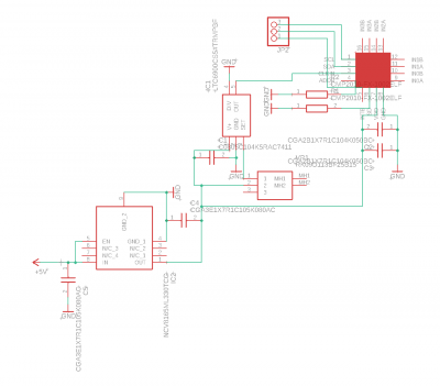
Now with a 5V to 3.3V converter with ultra-low noise output. With all these bypass capacitors this has to be a super-duper ultra-low noise circuit.
Just the Coils are missing (not that much work just a symbol with another capacitor in parallel). Then I have to design the PCB. I think I decided on making the prototype a 4 layer one. JLCs capabilities are just so much better with these then.
Had to take a break from this project. Now one and half months later I´m on it again. So nothing has changed. Still planning the 4-layer-PCB tho. The LDC1314 is a 4 channel chip, so I want to try out basically 4 different designs for PCB-Coils to evaluate which one is the best. Designs I want to try out (subject to change):
- 2 Real Layers on an otherwise 4 Layer PCB with a big via
- 2 Real Layers on an otherwise 4 Layer PCB without a big via
- 4 Real Layers on a 4 Layer PCB without a big via (because two are needed)
- 2 Real Layers on an otherwise 4 Layer PCB with a big via but with JLCs Capabilities for 2 Layer PCB
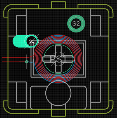
Here an example of design number 1 I made:
For the coils, I made some calculations, because there is a correlation between the frequency that is used and the needed capacitor in front of the coil.
Because of this I now know that I need the LTC6900 to output a frequency of roughly 6Mhz. Therefore I need to calculate the resistance of the resistor at the Set-Pin of the LTC6900. I calculated with this formula:
 N = 1
N = 1
So I need a 33.3kOhm resistor in front of the LTC6900 Set-Pin.
This (the LTC stuff above) will get “important” later, so you should read this article till the end.
And here is my first “final” schematic then:
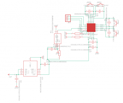
Btw I don't know how to make PCB-board-layouts. This can only get better.
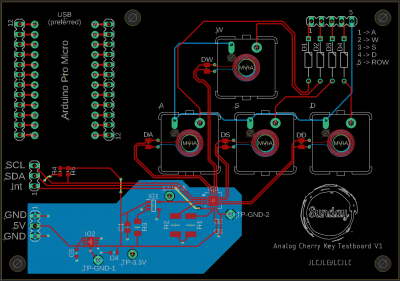
After I tried some designs I guess the only real option that is possible with the keys is Option Number 1 (2 Real Layers on an otherwise 4 Layer PCB with a big via). So I modified the Cherry Key Footprint to my likings and designed my first real PCB (kudos to Henrik). Here is V1 of the PCB:
I had some room left and also added a part where I can plug in an Arduino Pro Micro and connect to the real MX Key Pins.
So some time has past and I have waited nearly a month for my PCBs to arrive (because of customs). But they turned out great:

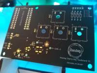
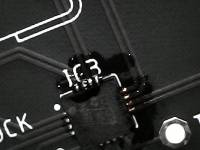
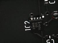
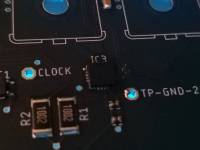
With a cheap microscope of eBay, I started inspecting the PCB. It´s stunning how tiny the coil traces are! With a “cheap” soldering station (with hot air) of eBay (eBay FTW ;D ) I made some test solders on a scrap PCB from the IoT-Lab with some very old soldering paste (also from the IoT-Lab). The paste wasn't really in a good condition, but mixed with Flux it worked great for me. When I kinda got the hang of soldering with hot air I started soldering the real PCB. So the first time hot air soldering with the first time QFN Soldering worked great. Not perfect, but the circuit works. Here are some close-ups:
And some more shots of the finished PCB:
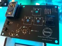
With the circuit finished I started working on the test code. My goal was to read out one of the coils and display the value on the serial plotter of the Arduino IDE. So more or less a proof of concept.
With the help of Google, I found a project by the GitHub-User dfieschko, in which he made an I2C library for the Teensy and the LDC1312/14 (Can be found here: LDC1312-Arduino). Because the library wasn't compatible with the Pro Micro I forked it and made my own version. The new library can be found here: LDC1312-Arduino. I didn't test all the functions but the ones I needed worked perfectly. I then started writing some code. And here is what came out:
- ldc1314-test.ino
#include <ldc1312_lib.h>
#include <Wire.h>

LDC131X ldc1314(false);
uint16_t lastTen[10];
int pointer;

void setup() {
  Wire.begin();
  Serial.begin(9600);
  ldc1314.LDC_resetLDC();
  delay(500);
  ldc1314.LDC_setConversionTime(0, 0x2000);
  ldc1314.LDC_setSettleTime(0, 0x000F);
  ldc1314.LDC_setClockDividers(0, 0x1002);
  ldc1314.LDC_setErrorConfig(0x0000);
  ldc1314.LDC_setDriveCurrent(0, 0xE800);
  ldc1314.LDC_setMUXConfig(0x20D);
  ldc1314.LDC_setGain(3);
  ldc1314.LDC_setOffset(0, 0x4FFF);
  ldc1314.LDC_setConfig(0x0801);

  pointer = 0;
}

void loop() {
  lastTen[pointer] = ldc1314.LDC_readData(0);
  pointer++;
  if (pointer > 9) {
    pointer = 0;
    int sum = 0;
    for(int i = 0; i < 9; i++) {
        sum += lastTen[i];
    }
    Serial.print("CH0 ");
    Serial.println(sum / 10);
  }
}
Let's go through this code step by step:
- Import the library and the Wire library (I2C)
- Then instantiate an LDC131X Object (the false means now alternative address)
- The lastTen and pointer variables are needed later to calculate an average of 10 measurements
- The setup starts with initiating the Wire and Serial communication
- Then the LDC gets a factory reset (the documentation states that this may need some milliseconds so I implemented a delay)
- On it goes with configuring the LDC (if the function accepts two arguments → the first one is the channel) (This is roughly done as described on page 48 of the documentation):
- ldc1314.LDC_setConversionTime(0, 0x2000)
- RCOUNT0
- 0x2000 → 10000000000000
- I set this to a higher value than actually needed because in this proof of concept I don't care about fast performance
- ldc1314.LDC_setSettleTime(0, 0x000F)
- SETTLECOUNT0
- 0x000F → 00000000001111
- SETTLECOUNT0 ≥ Q × fREF0 / (16 × fSENSOR0)
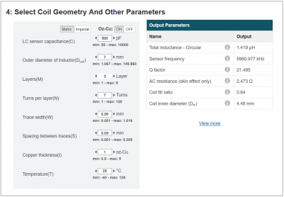
- Q = 21,495 (See the Webench screenshot)
- fREF0 = 43 Mhz
- fSENSOR0 = 5960,977 kHz ~ 6 Mhz (See the Webench screenshot)
- 8.9563 + Margin = 15
- ldc1314.LDC_setClockDividers(0, 0x1002)
- CLOCK_DIVIDERS0
- default
- FIN_DIVIDER0
- sensor frequency is less than 8.75MHz? → yes → 1
- FREF_DIVIDER0
- ƒREF0 is > 4 × ƒSENSOR
- 40Mhz > 4 x 6Mhz → reference Divider can be set to 1
- these two combine to 0x1002
- lookup page 21 of the documentation two see the register map for CLOCK_DIVIDERS0
- ldc1314.LDC_setErrorConfig(0x0000)
- ERROR_CONFIG
- default
- ldc1314.LDC_setDriveCurrent(0, 0xE800)
- DRIVE_CURRENT0
- I got the IDRIVE0 value from the table on page 40 of the documentation
- The best-fitting values (Nominal Sensor Current (μA), Minimum Sensor RP (kΩ), Maximum Sensor RP (kΩ)) where IDRIVEx Register Field Value 29 (b11101)
- INIT_DRIVE0 got set to 0
- combined 1110100000000000 → 0xE800
- ldc1314.LDC_setMUXConfig(0x20D)
- MUX_CONFIG
- 0x20D → 0000001000001101
- Auto-Scan Mode Enable → 0 → Continuous conversion on the single channel selected (0) (just testing with channel 0 right now)
- Auto-Scan Sequence Configuration → 00 → Ch0 + Ch1
- Input Deglitch Filter Bandwidth → 101 → 10 MHz (ƒSENSOR = 6 MHz)
- ldc1314.LDC_setGain(3)
- RESET_DEV
- 3 → 16x gain → 4 bits shift
- MOST IMPORTANT OPTION together with OFFSET. More about that later.
- ldc1314.LDC_setOffset(0, 0x4FFF)
- OFFSET0
- 0x4FFF → 100111111111111 (I know it's very high but that's needed)
- ldc1314.LDC_setConfig(0x0801)
- CONFIG
- 0x0801 → 0000100000000001
- Active Channel Selection → 00 → Perform continuous conversions on Channel 0
- Sleep Mode Enable → 0 → Device is active (This is important to set after configuring everything. Otherwise the device will stay in sleep mode.)
- Sensor RP Override Enable → 0 → Override off
- Sensor Activation Mode Selection → 1 → Low Power Activation Mode (made no difference for me right now)
- Automatic Sensor Amplitude Correction Disable → 0 → Automatic Amplitude correction enabled
- Select Reference Frequency Source → 0 → internal oscillator (More about this later)
- INTB Disable → 0
- High Current Sensor Drive → 0 → 1.5mA max per Channel
- After configuring all the settings the LDC is now active
- In the loop, I just read out the value of coil 0 (key D) and store the value in an array
- If I have ten readouts I calculate the average and print it on Serial
As I found out through trial and error, because of the fact that the coils are so tiny and the spring inside the switch isn't huge either, I needed a high gain and a high offset. An easy way to describe this is like using a magnifier and looking at a specific part of the value. But if you want to find out more about this topic, this document here really helped me: Optimizing L Measurement Resolution for the LDC1312 and LDC1314. Especially the pages 6 and 8 contain graphics that are really helpful. The whole document isn't that long and worth a read.
As you may have seen I set the LDC to not use the external oscillator I put on the PCB. This is because I miss understood the reason for this pin to exist. It´s an alternative to the internal oscillator. I thought I would have to put in the value I calculated for ƒSENSOR in Webench. That's why I have a 6Mhz input now. This is not needed! The LDC will compare the oscillating frequency that comes back from the coil (this is the 6MHz I calculated) with the internal oscillator (40 MHz) or a given external oscillator. But the oscillating frequency should be greater than 4 x 6MHz. Because this isn't the case with the one I got, I´m just using the internal one. This works so the external one does not have to be populated on the PCB. This also saves in cost on the final PCB. I hope this was understandable.

